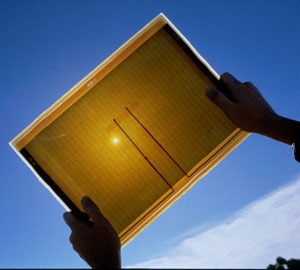
Researchers at the School of Photovoltaics and Renewable Energy Engineering (SPREE) at the University of New South Wales (UNSW) in Australia have developed an advanced processing technology for enhancing the efficiency of silicon solar cells. SPREE has entered into a research partnership with Suntech Power and Hanwha Solar, two major silicon solar cell manufacturers.

Thin film
The electric insulator in a solar cell is located between the aluminium back-plate and the silicon wafer. The newly developed technology involves “self-patterning” tiny metal contact regions into the electric insulator of a solar cell.
A senior lecturer at SPREE, Dr Alison Lennon, stated that, presently, laser scanning was being used for intentionally patterning holes in small-area metal contact regions that are closely-spaced in an insulating layer. However, this method is slow. Researchers have analysed other methods, including ink-jet and aerosol printing. These methods have not been able to deliver reliability in patterning and are also found to be quite slow.
SPREE researchers are considering aluminium anodisation for automating and increasing the speed of the patterning process. Anodisation of aluminium can be used for creating a porous insulating layer. This process is widely used in the metals processing industry for protection against corrosion.
The porous insulating layer is the target of this study. This will allow the aluminium layer to function as a dielectric layer having plenty of little holes. The UNSW researchers have presently produced prototypes of silicon solar cells with aluminium layers. They are now collaborating with Suntech Power and Hanwha Solar for improving the efficiencies of the cells to ensure commercial viability.
Disclaimer: The views expressed here are those of the author expressed in their private capacity and do not necessarily represent the views of AZoM.com Limited T/A AZoNetwork the owner and operator of this website. This disclaimer forms part of the Terms and conditions of use of this website.